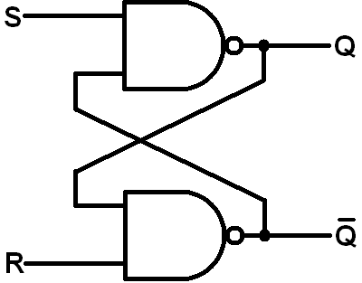
I started studying flip-flops recently and I am stuck at this point:
At some video tutorials, people explain the SR flip-flop like this:

So they use NAND gates, producing a transition table like this:
|     t     | t+1
|  S  |  R  |  Q

|  0  |  0  |  INVALID
|  0  |  1  |  1
|  1  |  0  |  0
|  1  |  1  |  ?
However, some other people explain the SR flip-flop using NOR gates:
SR2 http://startingelectronics.com/software/VHDL-CPLD-course/tut9-SR-latch/S-R-latch-gates.png
which has a different transition table.
Are both correct? Why do both exist?
Answer
Both are SR latches.
The SR NOR latch will have the following truth table:
----------
S  R   Q
----------
0  0   no change
0  1   0
1  0   1
1  1   not allowed
----------
SR NAND latch is an inverted version of SR NOR latch. The truth table of which is:
----------
S  R   Q
----------
0  0   not allowed
0  1   1
1  0   0
1  1   no change
----------
No comments:
Post a Comment